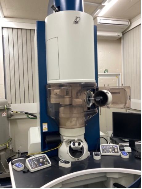
Atomic Resolution Analytical Electron microscopy (AEM)
Several kinds of analytical techniques equipped with atomic resolution scanning transmission electron microscope (STEM) make it possible to investigate local structure and physical properties of the sample with sub nano-meter resolution.
Application areas: Semiconductor, Battery, Nanomaterials, Metal
Strengths
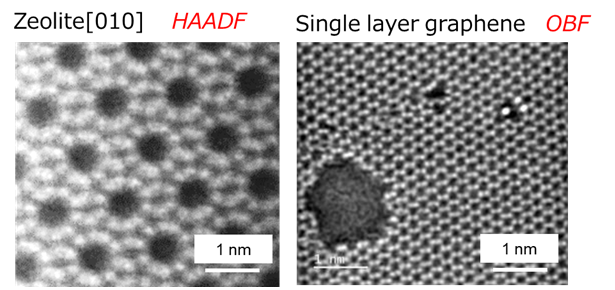
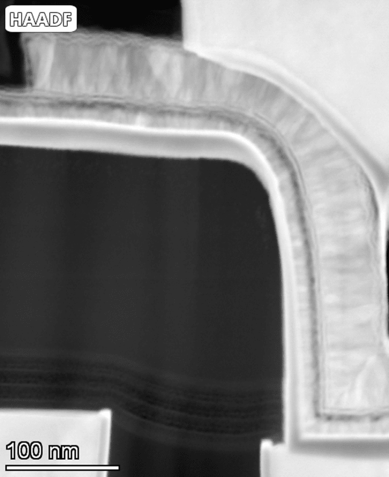
- New type spherical aberration corrector achieves 53 pm spatial resolution in STEM imaging.
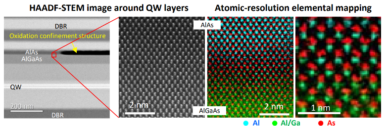
- Energy dispersive X-ray spectroscopy (EDX) with large solid-angle detectors can get information of elemental composition with high sensitivity.
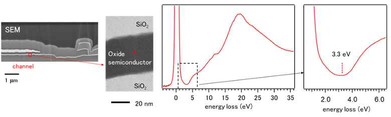
- 0.3 eV energy resolution EEL spectra (EELS) accompanied by highly skilled spectrum processing enable detailed investigation of electronic structure and optical properties.
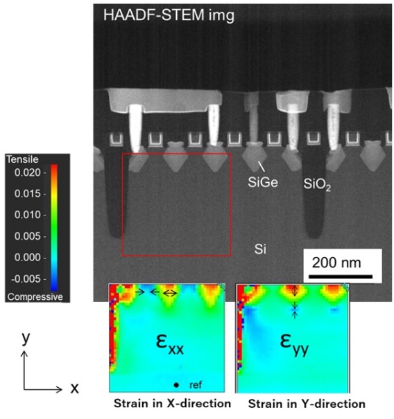
- Precession electron diffraction pattern series, ACOM (automated crystal orientation mapping)-TEM, can acquire the lattice strain mapping in an actual electronic device.
Limitations
- Thin lamella specimen preparation using ion-beam milling, which may cause sample damage but can be reduced by cryo-milling condition.
- Elemental composition analysis only for main components with the detection limit of 0.1 atom%.